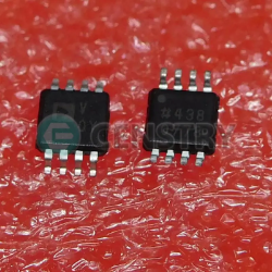
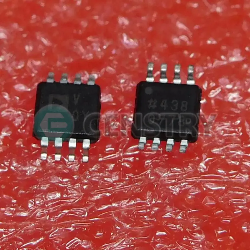
IC V/F CONV 1MHZ 8MSOP


画像は参考用です.
製品の詳細については、「製品仕様」を参照してください。
IC V/F CONV 1MHZ 8MSOP
200 ドル以上のご注文には、限定版の中華風のギフトがプレゼントされます.
1000 ドルを超える注文は、30 ドルの配送料免除の対象となります.
5000 ドルを超える注文では、配送料と取引手数料が免除されます.
これらのオファーは新規顧客と既存顧客の両方に適用され、2024 年 1 月 1 日から 2024 年 12 月 31 日まで有効です。.
ADI
AD7740YRMZ datasheet
MSOP8
ICチップ
 Lead free/RoHS Compliant
今すぐ見積もりリクエストを送信してください。3 日以内に見積もりを提出する予定です。 4月 21, 2024。 今すぐご注文ください。以内に取引が完了する予定です。 4月 25, 2024。 追伸:時間はGMT+8:00に従います。


FEATURES
Synchronous Operation
Full-Scale Frequency Set by External System Clock
8-Lead SOT-23 and 8-Lead microSOIC Packages
3 V or 5 V Operation
Low Power: 3 mW (Typ)
Nominal Input Range: 0 to VREF
True –150 mV Capability Without Charge Pump
VREF Range: 2.5 V to VDD
Internal 2.5 V Reference
1 MHz Max Input Frequency
Selectable High Impedance Buffered Input
Minimal External Components Required
APPLICATIONS
Isolation of High Common-Mode Voltages
Low-Cost Analog-to-Digital Conversion
Battery Monitoring
Automotive Sensing

GENERAL DESCRIPTION
The AD7740 is a low-cost, ultrasmall synchronous Voltage-toFrequency Converter (VFC). It works from a single 3.0 V to
3.6 V or 4.75 V to 5.25 V supply consuming 0.9 mA. The AD7740
is available in an 8-lead SOT-23 and also in an 8-lead microSOIC
package. Small package, low cost and ease of use were major
design goals for this product. The part contains an on-chip 2.5 V
bandgap reference but the user may overdrive this using an
external reference. This external reference range includes VDD.
The full-scale output frequency is synchronous with the clock
signal on the CLKIN pin. This clock can be generated with the
addition of an external crystal (or resonator) or supplied from a
CMOS-compatible clock source. The part has a maximum
input frequency of 1 MHz.
For an analog input signal that goes from 0 V to VREF, the output frequency goes from 10% to 90% of fCLKIN. In buffered mode,
the part provides a very high input impedance and accepts a
range of 0.1 V to VDD – 0.2 V on the VIN pin. There is also
an unbuffered mode of operation that allows VIN to go from
–0.15 V to VDD + 0.15 V. The modes are interchangeable using
the BUF pin.
The AD7740 (Y Grade) is guaranteed over the automotive
temperature range of –40°C to +105°C
PRODUCT HIGHLIGHTS
1. The AD7740 is a single channel, single-ended VFC. It is
available in 8-lead SOT-23 and 8-lead microSOIC packages,
and is intended for low-cost applications. The AD7740 offers
considerable space saving over alternative solutions.
2. The AD7740 operates from a single 3.0 V to 3.6 V or 4.75 V
to 5.25 V supply and consumes typically 0.9 mA when the
input is unbuffered. It also contains an automatic power-down
function.
3. The AD7740 does not require external resistors and capacitors to set the output frequency. The maximum output
frequency is set by a crystal or a clock. No trimming or calibration is required.
4. The analog input can be taken to 150 mV below GND for
true bipolar operation.
5. The specified voltage reference range on REFIN is from
2.5 V to the supply voltage, VDD.
Request a quote AD7740YRMZ at censtry.com. All items are new and original with 365 days warranty! The excellent quality
and guaranteed services of AD7740YRMZ in stock for sale, check stock quantity and pricing,
view product specifications, and order contact us:sales@censtry.com.
The price and lead time for AD7740YRMZ depending on the quantity required, please send your request to us,
our sales team will provide you price and delivery within 24 hours, we sincerely look forward to cooperating with you.
ZETEX
41 PCS
ZTX601B .PDF
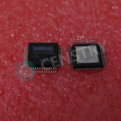
YAMAHA
384 PCS
YDA164C .PDF
YAMAHA
2000 PCS
YDA163C-SZE2 .PDF
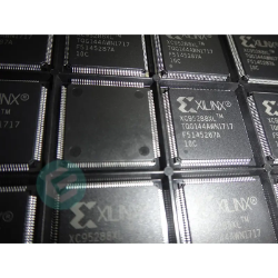
XILINX
2150 PCS
XC95288XL-10TQG144C .PDF
2024-04-20
Quick and Easy
2024-04-20
Great company and a long time customer, hope to continue for years and years more! ~Ngoc
2024-04-19
Great company to work with. Jim always honest and nice to work with. Will definitely do more business in the future.
2024-04-19
Great company. Quality product.
2024-04-17
Great supplier.
2024-04-15
Great product, fast delivery.
2024-04-09
Great Support.
2024-03-30
Have been dealing with Oliver for years and he always does a great job for us. Good pricing and delivery. Highly recommend
2024-03-08
Honest and Efficient company!!
2024-01-26
I HIGHLY RECOMMEND CENSTRY. MONKY IS GREAT TO WORK WITH - HE GETS BACK WITH ANSWERS QUICKLY. I WILL ADD HIM AS ONE OF MY PREFERRED VENDORS - KEEP UP THE GOOD WORK. BEATRICE
皆様からのフィードバックを非常に重視しております。 最も誠実なレビューを共有してください。
*コメントを投稿する前にアカウントにログインしてください