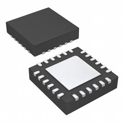
IC REG CONV DDR 1OUT 24WQFN


画像は参考用です.
製品の詳細については、「製品仕様」を参照してください。
IC REG CONV DDR 1OUT 24WQFN
200 ドル以上のご注文には、限定版の中華風のギフトがプレゼントされます.
1000 ドルを超える注文は、30 ドルの配送料免除の対象となります.
5000 ドルを超える注文では、配送料と取引手数料が免除されます.
これらのオファーは新規顧客と既存顧客の両方に適用され、2024 年 1 月 1 日から 2024 年 12 月 31 日まで有効です。.
TI
TPS54116QRTWRQ1 datasheet
WQFN-24
ICチップ
 Lead free/RoHS Compliant
今すぐ見積もりリクエストを送信してください。3 日以内に見積もりを提出する予定です。 4月 26, 2024。 今すぐご注文ください。以内に取引が完了する予定です。 5月 01, 2024。 追伸:時間はGMT+8:00に従います。


1 Features
• AEC-Q100 Qualified With the Following Results:
– Device Temperature Grade 1: –40°C to +125°C Ambient Operating Temperature Range
– Device HBM ESD Classification Level 2
– Device CDM ESD Classification Level C6
• Single-chip DDR2, DDR3 and DDR3L Memory Power Solution
• 4-A Synchronous Buck Converter
– Integrated 33-mΩ High-side and 25-mΩ Lowside MOSFETs
– Fixed Frequency Current-mode Control
– Adjustable Frequency from 100 kHz to 2.5 MHz
– Synchronizable to an External Clock
– 0.6-V ±1% Voltage Reference Over Temperature
– Adjustable Cycle-by-Cycle Peak Current Limit
– Monotonic Start-up Into Pre-biased Outputs
• 1-A Source/Sink Termination LDO with ±20-mV DC Accuracy
– Stable with 2 × 10-µF MLCC Capacitor
– 10-mA Source/Sink Buffered Reference Output Regulated to Within 49% to 51% of VDDQ
• Independent Enable Pins with Adjustable UVLO and Hysteresis
• Thermal Shutdown
• -40°C to 150°C Operating TJ
• 24-pin, 4-mm x 4-mm WQFN Package
2 Applications
• DDR2, DDR3, DDR3L, and DDR4 Memory Power Supplies in Embedded Computing Systems
• SSTL_18, SSTL_15, SSTL_135, SSTL_12 and HSTL Termination
• Infotainment and Cluster
• Advanced Driver Assistance Systems (ADAS)
3 Description
The TPS54116-Q1 device is a full featured 6-V, 4-A, synchronous step down converter with two integrated MOSFETs and 1-A sink/source double data rate (DDR) VTT termination regulator with VTTREF
buffered reference output.
The TPS54116-Q1 buck regulator minimizes solution size by integrating the MOSFETs and reducing inductor size with up to 2.5-MHz switching frequency. The switching frequency can be set above the medium wave radio band for noise sensitive applications and is synchronizable to an external clock. Synchronous rectification keeps the frequency fixed across the entire output load range. Efficiency is maximized through integrated 25-mΩ low-side and 33-mΩ high-side MOSFETs. Cycle-by-cycle peak current limit protects the device during an overcurrent condition and is adjustable with a resistor at the ILIM pin to optimize for smaller inductors.
The VTT termination regulator maintains fast transient response with only 2 × 10-µF ceramic output capacitance reducing external component count. The TPS54116-Q1 uses remote sensing of VTT for best regulation.
Using the enable pins to enter a shutdown mode reduces supply current to 1-µA. Under voltage
lockout thresholds can be set with a resistor network on either enable pin. The VTT and VTTREF outputs
are discharged when disabled with ENLDO. Full integration minimizes the IC footprint with a small
4 mm × 4 mm thermally enhanced WQFN package

Request a quote TPS54116QRTWRQ1 at censtry.com. All items are new and original with 365 days warranty! The excellent quality
and guaranteed services of TPS54116QRTWRQ1 in stock for sale, check stock quantity and pricing,
view product specifications, and order contact us:sales@censtry.com.
The price and lead time for TPS54116QRTWRQ1 depending on the quantity required, please send your request to us,
our sales team will provide you price and delivery within 24 hours, we sincerely look forward to cooperating with you.
ZETEX
41 PCS
ZTX601B .PDF
YAMAHA
384 PCS
YDA164C .PDF
YAMAHA
2000 PCS
YDA163C-SZE2 .PDF
XILINX
2150 PCS
XC95288XL-10TQG144C .PDF
2024-04-25
Jim is a pleasure to work with.
2024-04-25
Good supplier
2024-04-25
I will give a 5 star.
2024-04-24
It is a pleasure doing business with Censtry.
2024-04-23
GOOD COMUNICATION AND GOOD BIZ WE DID TOGETHER, WAITING FOR NEXT BIZ WITH THEM. BR ALBERT & ELVIN
2024-04-21
Good Honest Company. Thanks! Linda..
2024-04-17
Good quality and good service
2024-04-09
Good vendor,quality parts.Pearly is helpful and professional girl. wish do more biz with you.
2024-03-24
Great Company / Very Reliable
2024-02-21
Great company w/a great staff..Very easy to work with

皆様からのフィードバックを非常に重視しております。 最も誠実なレビューを共有してください。
*コメントを投稿する前にアカウントにログインしてください