SOT23-6 21+


画像は参考用です.
製品の詳細については、「製品仕様」を参照してください。
SOT23-6 21+
200 ドル以上のご注文には、限定版の中華風のギフトがプレゼントされます.
1000 ドルを超える注文は、30 ドルの配送料免除の対象となります.
5000 ドルを超える注文では、配送料と取引手数料が免除されます.
これらのオファーは新規顧客と既存顧客の両方に適用され、2024 年 1 月 1 日から 2024 年 12 月 31 日まで有効です。.
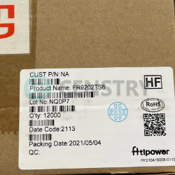
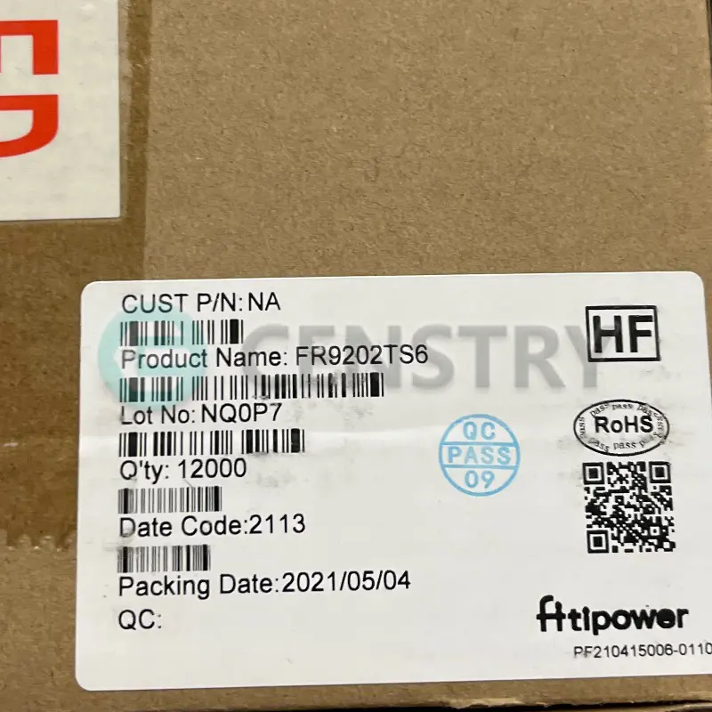
FITIPOWER
FR9202TS6 datasheet
SOT23-6
RF集積回路
 Lead free/RoHS Compliant
今すぐ見積もりリクエストを送信してください。3 日以内に見積もりを提出する予定です。 5月 01, 2024。 今すぐご注文ください。以内に取引が完了する予定です。 5月 06, 2024。 追伸:時間はGMT+8:00に従います。


1 FEATURES
◆ 64M-bit Serial Flash ◆ Fast Program/Erase Speed
- 8192K-Byte - Page Program time: 0.5ms typical
- 256 Bytes per programmable page - Sector Erase time: 45ms typical
- Block Erase time: 0.15s/0.25s typical
◆ Standard, Dual, Quad SPI - Chip Erase time: 25s typical
- Standard SPI: SCLK, CS#, SI, SO, WP#, HOLD#
- Dual SPI: SCLK, CS#, IO0, IO1, WP#, HOLD# ◆ Flexible Architecture
- Quad SPI: SCLK, CS#, IO0, IO1, IO2, IO3 - Uniform Sector of 4K-Byte
- Uniform Block of 32/64K-Byte
◆ High Speed Clock Frequency
- 133MHz for fast read ◆ Low Power Consumption
- Dual I/O Data transfer up to 266Mbits/s - 12μA typical standby current
- Quad I/O Data transfer up to 532Mbits/s - 1μA typical deep power down current
◆ Software/Hardware Write Protection ◆ Advanced Security Features
- Write protect all/portion of memory via software - 128-bit Unique ID for each device
- Enable/Disable protection with WP# Pin - Serial Flash Discoverable parameters (SFDP) register
- Top/Bottom Block protection - 3x1024-Byte Security Registers With OTP Locks
◆ Endurance and Data Retention ◆ Single Power Supply Voltage
- Minimum 100,000 Program/Erase Cycles - Full voltage range: 2.7-3.6V
- 20-year data retention typical
◆ Package Information
◆ Allows XiP (eXecute In Place) Operation - SOP8 150mil
- High speed Read reduce overall XiP instruction fetch time - SOP8 208mil
- Continuous Read with Wrap further reduce data latency to - SOP16 300mil
fill up SoC cache - USON8 (3x4mm)
- USON8 (4x4mm)
- WSON8 (6x5mm)
- WSON8 (8x6mm)
- TFBGA-24ball (4x6 Ball Array)
- TFBGA-24ball (5x5 Ball Array)
2 GENERAL DESCRIPTIONS
The GD25Q64E (64M-bit) Serial flash supports the standard Serial Peripheral Interface (SPI), and the Dual/Quad SPI:
Serial Clock, Chip Select, Serial Data I/O0 (SI), I/O1 (SO), I/O2 (WP#), I/O3 (HOLD#). The Dual I/O data is transferred
with speed of 266Mbit/s, and the Quad I/O data is transferred with speed of 532Mbit/s.
CONNECTION DIAGRAM

Request a quote FR9202TS6 at censtry.com. All items are new and original with 365 days warranty! The excellent quality
and guaranteed services of FR9202TS6 in stock for sale, check stock quantity and pricing,
view product specifications, and order contact us:sales@censtry.com.
The price and lead time for FR9202TS6 depending on the quantity required, please send your request to us,
our sales team will provide you price and delivery within 24 hours, we sincerely look forward to cooperating with you.
FUJI
1 PCS
7MBP75VFN060-52 .PDF
ABLIC
7692 PCS
S-93L76AD0I-T8T1G .PDF
ABLIC
7764 PCS
S-93L76AD0I-J8T1G .PDF
ABLIC
7708 PCS
S-93L66AR0I-J8T1G .PDF
2024-04-30
Components worked fine. Pleased with purchases.
2024-04-30
THANK YOU.....I GOT THE ITEM QUICKLY.
2024-04-29
every things ok!!!
2024-04-29
Thanks for everything, everything came together very well
2024-04-27
I hope the chips match the description. Thank!
2024-04-25
All the parts worked good
2024-04-19
Years of good business and service, great team of people!
2024-04-09
we paid in advance and received good product, smooth transaction. no headaches. Hardy
2024-03-18
We compliment the team at Censtry for their hard work, quick payments, and all of the successful orders processed over the years! Thank you!
2024-02-05
Very reliable source. Looking forward to do more business with Oliver.
皆様からのフィードバックを非常に重視しております。 最も誠実なレビューを共有してください。
*コメントを投稿する前にアカウントにログインしてください