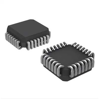
Clock Drivers & Distribution ISP 0 Delay Unv Fan- Out Buf-Sngl End I


画像は参考用です.
製品の詳細については、「製品仕様」を参照してください。
Clock Drivers & Distribution ISP 0 Delay Unv Fan- Out Buf-Sngl End I
200 ドル以上のご注文には、限定版の中華風のギフトがプレゼントされます.
1000 ドルを超える注文は、30 ドルの配送料免除の対象となります.
5000 ドルを超える注文では、配送料と取引手数料が免除されます.
これらのオファーは新規顧客と既存顧客の両方に適用され、2024 年 1 月 1 日から 2024 年 12 月 31 日まで有効です。.
Lattice
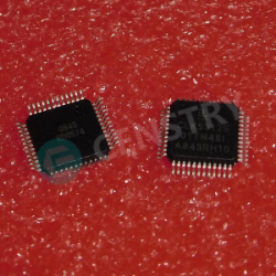
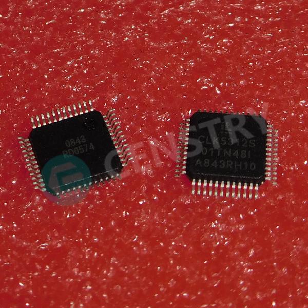
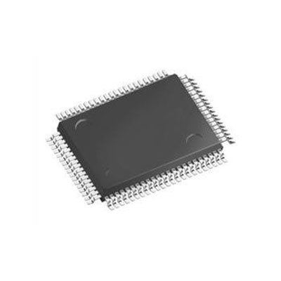
ISPPAC-CLK5312S-01TN48I datasheet
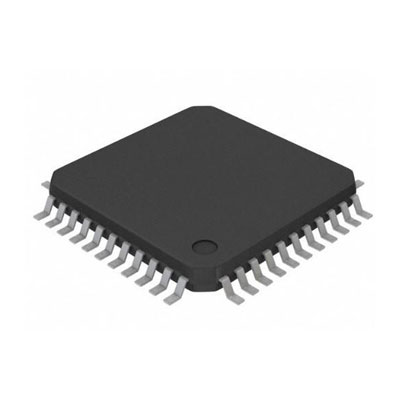
QFP-48
時計とタイマーIC
今すぐ見積もりリクエストを送信してください。3 日以内に見積もりを提出する予定です。 5月 03, 2024。 今すぐご注文ください。以内に取引が完了する予定です。 5月 08, 2024。 追伸:時間はGMT+8:00に従います。


Features
■ Four Operating Configurations
• Zero delay buffer
• Zero delay and non-zero delay buffer
• Dual non-zero delay buffer
• Non-zero delay buffer with output divider
■ 8MHz to 267MHz Input/Output Operation
■ Low Output to Output Skew (<100ps)
■ Low Jitter Peak-to-Peak (< 70 ps)
■ Up to 20 Programmable Fan-out Buffers
• Programmable single-ended output standards and individual enable controls
- LVTTL, LVCMOS, HSTL, eHSTL, SSTL
• Programmable output impedance
- 40 to 70Ω in 5Ω increments
• Programmable slew rate
• Up to 10 banks with individual VCCO and GND
- 1.5V, 1.8V, 2.5V, 3.3V
■ Fully Integrated High-Performance PLL
• Programmable lock detect
• Three “Power of 2” output dividers (5-bit)
• Programmable on-chip loop filter
• Compatible with spread spectrum clocks
• Internal/external feedback
■ Precision Programmable Phase Adjustment (Skew) Per Output
• 8 settings; minimum step size 156ps
- Locked to VCO frequency
• Up to +/- 5ns skew range
• Coarse and fine adjustment modes
■ Up to Three Clock Frequency Domains
■ Flexible Clock Reference and External Feedback Inputs
• Programmable single-ended or differential input reference standards
- LVTTL, LVCMOS, SSTL, HSTL, LVDS, LVPECL, Differential HSTL, Differential SSTL
• Clock A/B selection multiplexer
• Programmable Feedback Standards
- LVTTL, LVCMOS, SSTL, HSTL
• Programmable termination
■ All Inputs and Outputs are Hot Socket Compliant
■ Full JTAG Boundary Scan Test In-System Programming Support
■ Exceptional Power Supply Noise Immunity
■ Commercial (0 to 70°C) and Industrial (-40 to 85°C) Temperature Ranges
■ 48-pin and 64-pin TQFP Packages
■ Applications
• Circuit board common clock distribution
• PLL-based frequency generation
• High fan-out clock buffer
• Zero-delay clock buffer
General Description
The ispClock5300S is an in-system-programmable zero delay universal fan-out buffer for use in clock distribution applications. The ispClock5312S, the first member of the ispClock5300S family, provides up to 12 single-ended ultra low skew outputs. Each pair of outputs may be independently configured to support separate I/O standards (LVTTL, LVCMOS -3.3V, 2.5V, 1.8, SSTL, HSTL) and output frequency. In addition, each output provides independent programmable control of termination, slew-rate, and timing skew. All configuration information is stored onchip in non-volatile E2 CMOS® memory.
The ispClock5300S devices provide extremely low propagation delay (zero-delay) from input to output using the on-chip low jitter high-performance PLL. A set of three programmable 5-bit counters can be used to generate three frequencies derived from the PLL clock. These counters are programmable in powers of 2 only (1, 2, 4, 8, 16, 32). The clock output from any of the V-dividers can then be routed to any clock output pin through the output routing matrix. The output routing matrix, in addition, also enables routing of reference clock inputs directly to any output.

Request a quote ISPPAC-CLK5312S-01TN48I at censtry.com. All items are new and original with 365 days warranty! The excellent quality
and guaranteed services of ISPPAC-CLK5312S-01TN48I in stock for sale, check stock quantity and pricing,
view product specifications, and order contact us:sales@censtry.com.
The price and lead time for ISPPAC-CLK5312S-01TN48I depending on the quantity required, please send your request to us,
our sales team will provide you price and delivery within 24 hours, we sincerely look forward to cooperating with you.
Lattice
147 PCS
A5-64/32-10VC-10VI .PDF
Lattice
9 PCS
5962-9308501MXC .PDF
Lattice
4 PCS
1M4A5-64/32 7JC-10JI .PDF
Lattice
55 PCS
1M4A3-96/48 .PDF
2024-05-02
Great Team!!
2024-05-02
Great parts , great price , great service.
2024-05-02
Great supplier over the year!!! we love Gil, Ed, and Karen there.......
2024-05-01
Haim is a great salesperson, one of the best around! Heather Fisher
2024-04-30
It is a pleasure doing business with Censtry.
2024-04-28
I hope we can do more buisness in the Future.
2024-04-24
It was a pleasure to work with Susan at Censtry. Thank you
2024-04-16
John Walsh is great to work and is very professional.
2024-03-31
Kevin fast shipper ,RECOMMENDED !
2024-02-28
Lizzeth was a joy to work with.

皆様からのフィードバックを非常に重視しております。 最も誠実なレビューを共有してください。
*コメントを投稿する前にアカウントにログインしてください