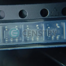
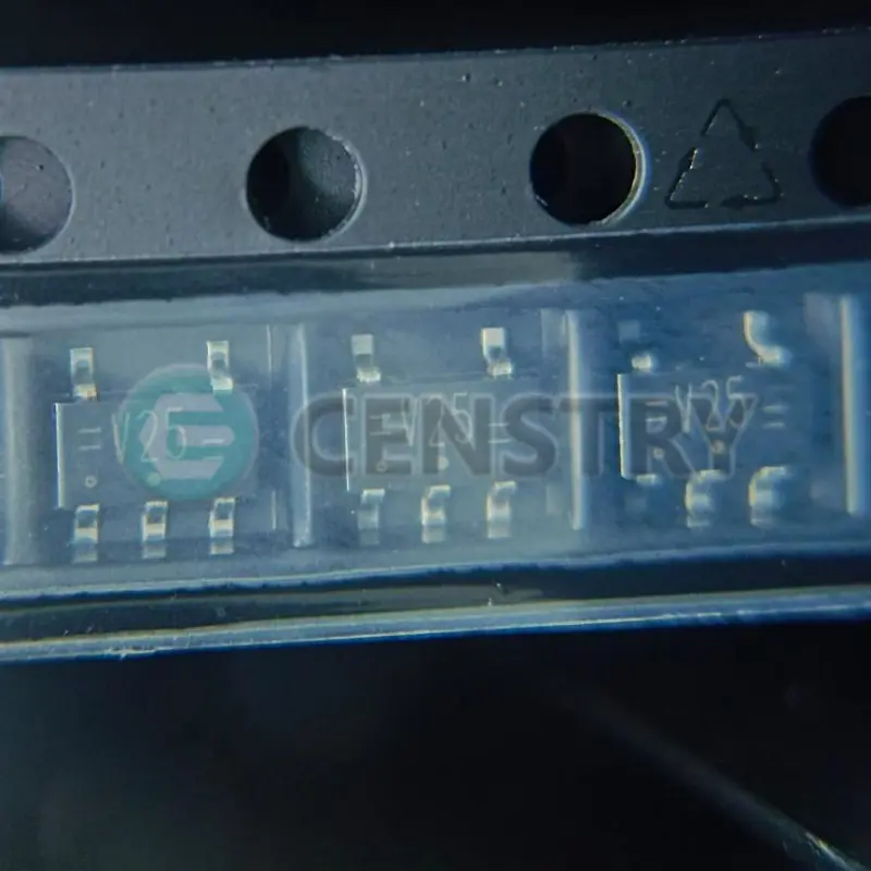
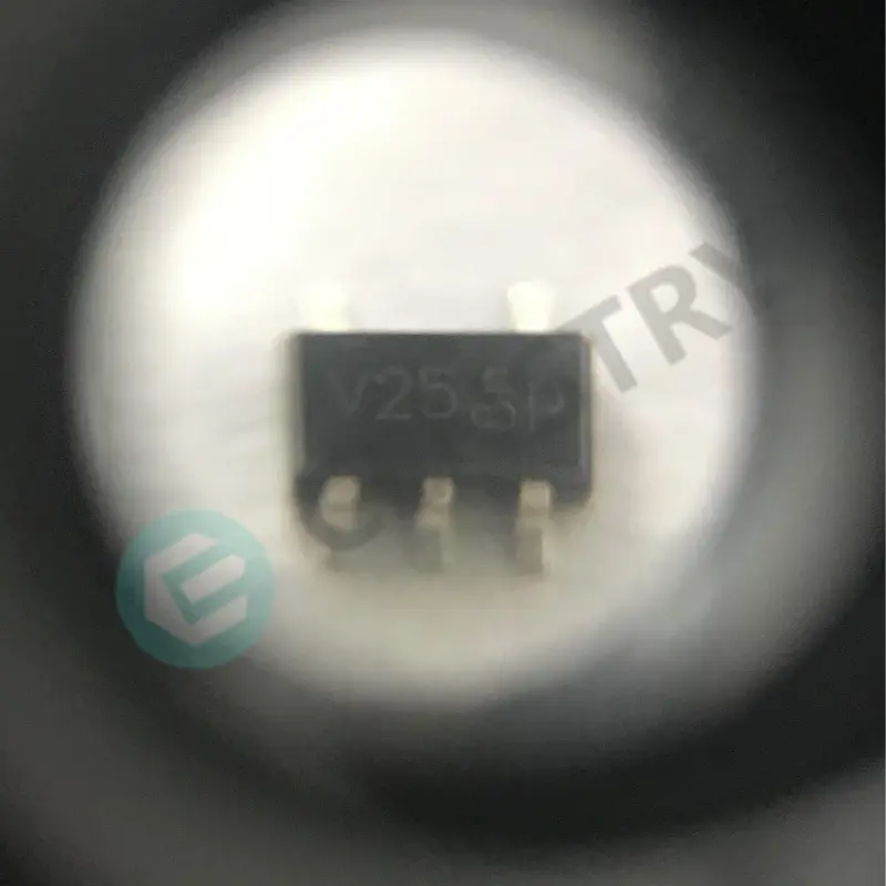
IC BUFFER NON-INVERT 5.5V SC74A


画像は参考用です.
製品の詳細については、「製品仕様」を参照してください。
IC BUFFER NON-INVERT 5.5V SC74A
200 ドル以上のご注文には、限定版の中華風のギフトがプレゼントされます.
1000 ドルを超える注文は、30 ドルの配送料免除の対象となります.
5000 ドルを超える注文では、配送料と取引手数料が免除されます.
これらのオファーは新規顧客と既存顧客の両方に適用され、2024 年 1 月 1 日から 2024 年 12 月 31 日まで有効です。.
NXP
74LVC1G125GV datasheet
SOT753
ICチップ
 Lead free/RoHS Compliant
今すぐ見積もりリクエストを送信してください。3 日以内に見積もりを提出する予定です。 5月 03, 2024。 今すぐご注文ください。以内に取引が完了する予定です。 5月 07, 2024。 追伸:時間はGMT+8:00に従います。


FEATURES
• Wide supply voltage range from 1.65 V to 5.5 V
• High noise immunity
• Complies with JEDEC standard:
– JESD8-7 (1.65 V to 1.95 V)
– JESD8-5 (2.3 V to 2.7 V)
– JESD8B/JESD36 (2.7 V to 3.6 V).
• ±24 mA output drive (VCC = 3.0 V)
• CMOS low power consumption
• Latch-up performance exceeds 250 mA
• Direct interface with TTL levels
• Inputs accept voltages up to 5 V
• Multiple package options
• ESD protection:
– HBM EIA/JESD22-A114-B exceeds 2000 V
– MM EIA/JESD22-A115-A exceeds 200 V.
• Specified from −40 °C to +85 °C and −40 °C to +125 °C.
DESCRIPTION
The 74LVC1G125 is a high-performance, low-power,
low-voltage, Si-gate CMOS device, superior to most
advanced CMOS compatible TTL families.
The input can be driven from either 3.3 V or 5 V devices.
This feature allows the use of this device in a mixed
3.3 V and 5 V environment.
This device is fully specified for partial power-down
applications using Ioff. The Ioff circuitry disables the output,
preventing the damaging backflow current through the
device when it is powered down.
The 74LVC1G125 provides one non-inverting buffer/line
driver with 3-state output. The 3-state output is controlled
by the output enable input (OE). A HIGH level at pin OE
causes the output to assume a high-impedance
OFF-state.


Request a quote 74LVC1G125GV at censtry.com. All items are new and original with 365 days warranty! The excellent quality
and guaranteed services of 74LVC1G125GV in stock for sale, check stock quantity and pricing,
view product specifications, and order contact us:sales@censtry.com.
The price and lead time for 74LVC1G125GV depending on the quantity required, please send your request to us,
our sales team will provide you price and delivery within 24 hours, we sincerely look forward to cooperating with you.
FUJI
1 PCS
7MBP75VFN060-52 .PDF
ABLIC
7692 PCS
S-93L76AD0I-T8T1G .PDF
ABLIC
7764 PCS
S-93L76AD0I-J8T1G .PDF
ABLIC
7708 PCS
S-93L66AR0I-J8T1G .PDF
2024-05-02
Excellent supplier- George and Andy are true closers - Thanks for the business!
2024-05-02
Fast and reliable company
2024-05-01
Fast service, fair price and good product, thank you.
2024-05-01
Gabi is easy to deal with. Parts came in on time. Will deal with again. Gretchen
2024-05-01
Good and reliable company
2024-04-30
Quick and Easy
2024-04-29
Good company, excellent sales
2024-04-26
Good cooperation
2024-04-21
Good part , all good .
2024-04-10
Good service and good parts

皆様からのフィードバックを非常に重視しております。 最も誠実なレビューを共有してください。
*コメントを投稿する前にアカウントにログインしてください