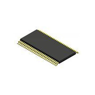
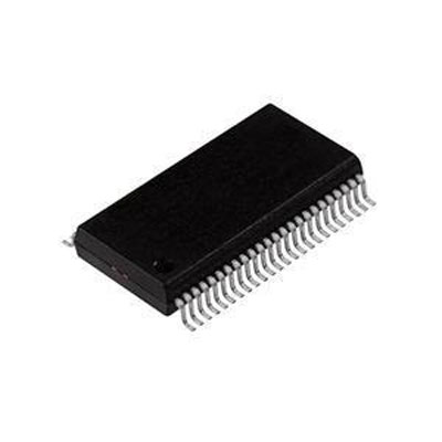
LVDS Interface IC LVDS Serder Receiver


画像は参考用です.
製品の詳細については、「製品仕様」を参照してください。
LVDS Interface IC LVDS Serder Receiver
200 ドル以上のご注文には、限定版の中華風のギフトがプレゼントされます.
1000 ドルを超える注文は、30 ドルの配送料免除の対象となります.
5000 ドルを超える注文では、配送料と取引手数料が免除されます.
これらのオファーは新規顧客と既存顧客の両方に適用され、2024 年 1 月 1 日から 2024 年 12 月 31 日まで有効です。.
TI
N65LVDS94 datasheet
TSSOP-56
RF集積回路
今すぐ見積もりリクエストを送信してください。3 日以内に見積もりを提出する予定です。 5月 09, 2024。 今すぐご注文ください。以内に取引が完了する予定です。 5月 14, 2024。 追伸:時間はGMT+8:00に従います。


TI
115 PCS
AML3501 .PDF
TI
30 PCS
AMI808EZWT .PDF
TI
40 PCS
AMI808BZWT .PDF
TI
184 PCS
AM3352BZCZD30 .PDF
2024-05-08
Jim is a pleasure to work with.
2024-05-08
Easy to deal with. Kenny is a great guy.
2024-05-07
Excellent company - Thank you for your help
2024-05-07
Excellent Team
2024-05-05
Great company, highly recommended A+++++
2024-05-02
First time order went very well, excellent service, quality product
2024-04-25
GOOD SUPPLIER FROM 2 YEARS.
2024-04-12
Good Company
2024-03-16
Good company! Good payment! hope to do business with you again!!
2024-01-23
Good Company. Nice to work with.
皆様からのフィードバックを非常に重視しております。 最も誠実なレビューを共有してください。
*コメントを投稿する前にアカウントにログインしてください