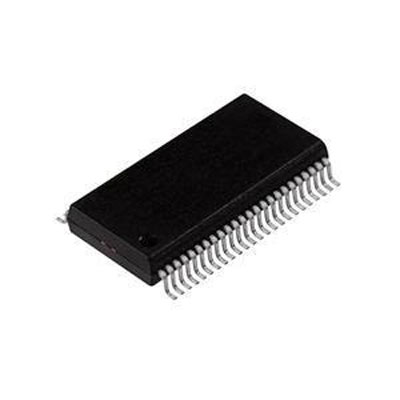
IC PWR SWITCH N-CHAN 1:1 SOT23-6


画像は参考用です.
製品の詳細については、「製品仕様」を参照してください。
IC PWR SWITCH N-CHAN 1:1 SOT23-6
200 ドル以上のご注文には、限定版の中華風のギフトがプレゼントされます.
1000 ドルを超える注文は、30 ドルの配送料免除の対象となります.
5000 ドルを超える注文では、配送料と取引手数料が免除されます.
これらのオファーは新規顧客と既存顧客の両方に適用され、2024 年 1 月 1 日から 2024 年 12 月 31 日まで有効です。.
TI
TPS22810TDBVRQ1 datasheet
SOT23-6
ICチップ
 Lead free/RoHS Compliant
今すぐ見積もりリクエストを送信してください。3 日以内に見積もりを提出する予定です。 5月 04, 2024。 今すぐご注文ください。以内に取引が完了する予定です。 5月 09, 2024。 追伸:時間はGMT+8:00に従います。


1 Features
• Qualified for Automotive Applications
• AEC-Q100 Qualified With the Following Results:
– Device Temperature Grade 2: –40°C to +105°C Ambient Operating Temperature
– Device HBM ESD Classification Level 2
– Device CDM ESD Classification Level C5
• Integrated Single Channel Load Switch
• 2-A Maximum Continuous Current
• Input Voltage: 2.7 V to 18 V
• Absolute Maximum Input Voltage: 20 V
• On-Resistance (RON)
– RON = 79 mΩ (Typical) at VIN = 12 V
• Quiescent Current
– 62 µA (Typical) at VIN = 12 V
• Shutdown Current
– 500 nA (Typical) at VIN = 12 V
• Thermal Shutdown
• Undervoltage Lock-Out (UVLO)
• Adjustable Quick Output Discharge (QOD)
• Configurable Rise Time With CT Pin
• SOT23-6 Package
– 2.9-mm × 2.8-mm, 0.95-mm Pitch,
1.45-mm Height (DBV)
2 Applications
• Automotive Head Unit
• Surround View ECU
3 Description
The TPS22810-Q1 is a one channel load switch with configurable rise time and integrated quick output discharge (QOD). The device features thermalshutdown to protect the device against high junction temperature and thereby ensure safe operating area of the device inherently. The device features a Nchannel MOSFET that can operate over an input voltage range of 2.7 V to 18 V. The device can support a maximum current of 2 A. The switch is controlled by an on and off input that can interface directly with low-voltage control signals.
The configurable rise time of the device greatly reduces inrush current caused by large bulk load capacitances, thereby reducing or eliminating power supply droop. Undervoltage lock-out is used to turn off the device if the VIN voltage drops below a threshold value, ensuring that the downstream circuitry is not damaged by being supplied by a voltage lower than intended. The configurable QOD pin controls the fall time of the device to allow design flexibility for power down.
The TPS22810-Q1 is available in a leaded, SOT-23 package (DBV) which allows to visually inspect solder joints. The device is characterized for operation over the free-air temperature range of –40˚C to +105˚C.

Request a quote TPS22810TDBVRQ1 at censtry.com. All items are new and original with 365 days warranty! The excellent quality
and guaranteed services of TPS22810TDBVRQ1 in stock for sale, check stock quantity and pricing,
view product specifications, and order contact us:sales@censtry.com.
The price and lead time for TPS22810TDBVRQ1 depending on the quantity required, please send your request to us,
our sales team will provide you price and delivery within 24 hours, we sincerely look forward to cooperating with you.


TI
115 PCS
AML3501 .PDF
TI
30 PCS
AMI808EZWT .PDF
TI
40 PCS
AMI808BZWT .PDF
TI
184 PCS
AM3352BZCZD30 .PDF
2024-05-03
very fast thanks
2024-05-03
Fast shipping
2024-05-02
Goods arrived and work perfectly.
2024-05-02
impossible to find, except here.
2024-04-30
TRANSISTORS ARE GOOD
2024-04-28
Mercancía correcta. Envío rápido. Muy satisfecho.
2024-04-22
Censtry elec = Good company, happy business
2024-04-12
We highly recommend Pinewood Electronics Ltd and are looking forward to our next deal. Darren is very professional and our order was shipped promptly and the parts were good quality.
2024-03-21
Good supplier !i will buy it again ,Nice
2024-02-08
Very proffessional and reliable company. Was a pleasure for me to work with Mara.

皆様からのフィードバックを非常に重視しております。 最も誠実なレビューを共有してください。
*コメントを投稿する前にアカウントにログインしてください