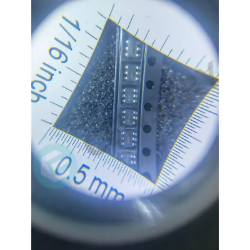
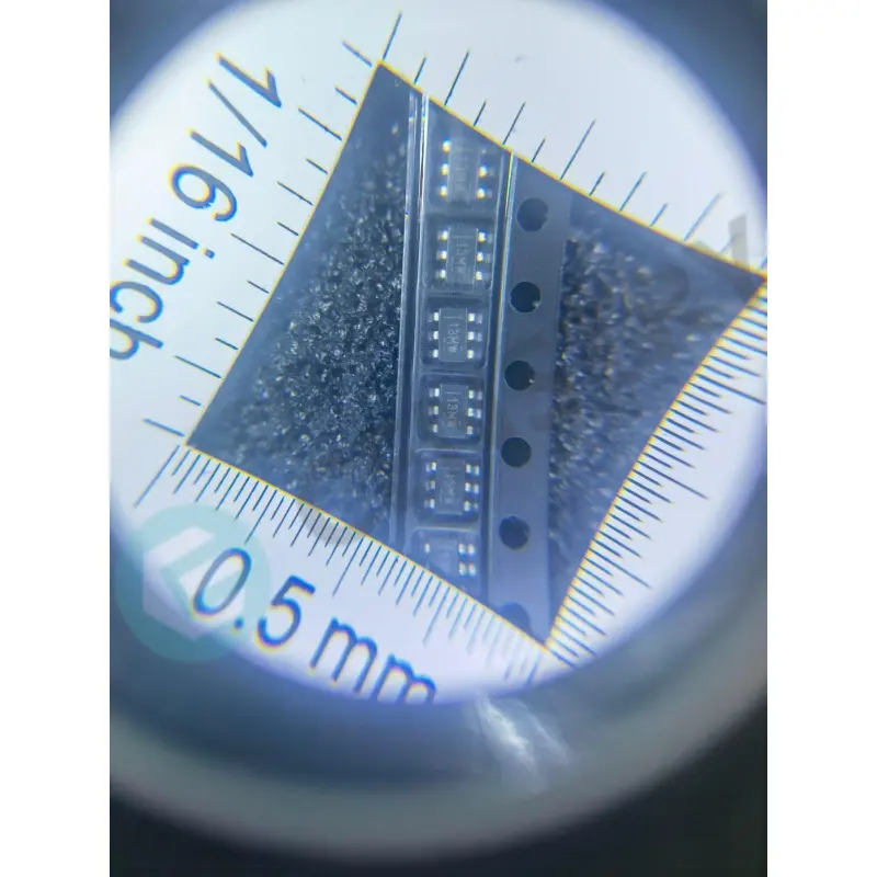
Power Switch/Driver 1:1 N-Channel 2A SOT-23-6


画像は参考用です.
製品の詳細については、「製品仕様」を参照してください。
Power Switch/Driver 1:1 N-Channel 2A SOT-23-6
200 ドル以上のご注文には、限定版の中華風のギフトがプレゼントされます.
1000 ドルを超える注文は、30 ドルの配送料免除の対象となります.
5000 ドルを超える注文では、配送料と取引手数料が免除されます.
これらのオファーは新規顧客と既存顧客の両方に適用され、2024 年 1 月 1 日から 2024 年 12 月 31 日まで有効です。.
TI
TPS22918DBVR datasheet
SOT-23-6
ICチップ
 Lead free/RoHS Compliant
今すぐ見積もりリクエストを送信してください。3 日以内に見積もりを提出する予定です。 4月 30, 2024。 今すぐご注文ください。以内に取引が完了する予定です。 5月 03, 2024。 追伸:時間はGMT+8:00に従います。


1 Features
• Integrated Single Channel Load Switch
• Ambient Operating Temperature: –40°C to +105°C
• Input Voltage Range: 1 V to 5.5 V
• On-Resistance (RON)
– RON = 52 mΩ (typical) at VIN = 5 V
– RON = 53 mΩ (typical) at VIN = 3.3 V
• 2-A Maximum Continuous Switch Current
• Low Quiescent Current
– 8.3 µA (typical) at VIN = 3.3 V
• Low-Control Input-Threshold Enables Use of 1 V or Higher GPIO
• Adjustable Quick-Output Discharge (QOD)
• Configurable Rise Time With CT Pin
• Small SOT23-6 Package (DBV)
– 2.90-mm × 2.80-mm, 0.95-mm Pitch,
1.45 mm Height (with leads)
• ESD Performance Tested per JESD 22
– ±2-kV HBM and ±1-kV CDM
2 Applications
• Industrial Systems
• Set Top Box
• Blood Glucose Meters
• Electronic Point of Sale
3 Description
The TPS22918 is a single-channel load switch with configurable rise time and configurable quick output discharge. The device contains an N-channel MOSFET that can operate over an input voltage range of 1 V to 5.5 V and can support a maximum continuous current of 2 A. The switch is controlled by an on and off input, which is capable of interfacing directly with low-voltage control signals.
The configurable rise time of the device greatly reduces inrush current caused by large bulk load capacitances, thereby reducing or eliminating power supply droop. The TPS22918 features a configurable quick output discharge (QOD) pin, which controls the fall time of the device to allow design flexibility for power down and sequencing.
The TPS22918 is available in a small, leaded SOT-23 package (DBV) which allows visual inspection of solder joints. The device is characterized for operation over the free-air temperature range of –40°C to +105°C.

Request a quote TPS22918DBVR at censtry.com. All items are new and original with 365 days warranty! The excellent quality
and guaranteed services of TPS22918DBVR in stock for sale, check stock quantity and pricing,
view product specifications, and order contact us:sales@censtry.com.
The price and lead time for TPS22918DBVR depending on the quantity required, please send your request to us,
our sales team will provide you price and delivery within 24 hours, we sincerely look forward to cooperating with you.
TI
115 PCS
AML3501 .PDF
TI
30 PCS
AMI808EZWT .PDF
TI
40 PCS
AMI808BZWT .PDF
TI
184 PCS
AM3352BZCZD30 .PDF
2024-04-29
A company you can trust
2024-04-29
Louis is the most friendly and very professional supplier Great to work with him!
2024-04-29
Censtry is easy to work with!Will recommend to all~ Nice itemsThanks
2024-04-29
never Problems, fast Response, fair Prices. Thanks Kim
2024-04-28
CENSTRY is a great guy,good company very reliableParts receive on time!!!
2024-04-28
Original parts. Fast shippment.
2024-04-26
Perfect biz
2024-04-24
Reliable company ,good price ,original items ,i will buy again ,recommended !!
2024-04-18
Professional Supplier
2024-04-08
Quick reply, reliable Company

皆様からのフィードバックを非常に重視しております。 最も誠実なレビューを共有してください。
*コメントを投稿する前にアカウントにログインしてください