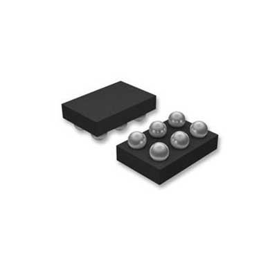
Power Switch/Driver 1:1 N-Channel 3A 6-DSBGA


画像は参考用です.
製品の詳細については、「製品仕様」を参照してください。
Power Switch/Driver 1:1 N-Channel 3A 6-DSBGA
200 ドル以上のご注文には、限定版の中華風のギフトがプレゼントされます.
1000 ドルを超える注文は、30 ドルの配送料免除の対象となります.
5000 ドルを超える注文では、配送料と取引手数料が免除されます.
これらのオファーは新規顧客と既存顧客の両方に適用され、2024 年 1 月 1 日から 2024 年 12 月 31 日まで有効です。.
TI
TPS22925CNYPHR datasheet
DSBGA-6
RF集積回路
 Lead free/RoHS Compliant
今すぐ見積もりリクエストを送信してください。3 日以内に見積もりを提出する予定です。 5月 05, 2024。 今すぐご注文ください。以内に取引が完了する予定です。 5月 08, 2024。 追伸:時間はGMT+8:00に従います。


1 Features
• Input Voltage Range: 0.65 V to 3.6 V
• On-Resistance
– RON = 9.2 mΩ at VIN = 3.6 V
– RON = 9.2 mΩ at VIN = 1.8 V
– RON = 10.2 mΩ at VIN = 1 V
– RON = 13.1 mΩ at VIN = 0.65 V
• 3-A Maximum Continuous Switch Current
• Quiescent Current, IQ,VIN = 29 µA at VIN = 3.6 V
• Low Control Input Threshold Enables 1.5-, 1.8-, 2.5-, or 3.3-V Logic
• Controlled Slew Rate
– tR = 97 µs at VIN = 3.6 V (TPS22925Bx)
– tR = 810 µs at VIN = 3.6 V (TPS22925Cx)
• Reverse Current Blocking (When Disabled)
• Quick Output Discharge (QOD) (TPS22925B and TPS22925C only)
• Wafer Chip Scale Package:
– 0.9 mm x 1.4 mm, 0.5-mm Pitch, 0.4-mm Height
• ESD Performance Tested per JESD 22
– 2-kV HBM and 1-kV CDM
2 Applications
• Computing
• SSD
• Tablets
• Wearables
• EPOS
3 Description
The TPS22925 product family consists of four devices: TPS22925B, TPS22925BN, TPS22925C,
and TPS22925CN. Each device is a 9-mΩ, singlechannel load switch with a controlled slew rate.
The devices contain an N–channel MOSFET that can operate over an input voltage range of 0.65 V to 3.6 V and can support a maximum continuous current of 3 A. This continuous current enables the devices to be used across multiple designs and end equipments. Each of the TPS22925 devices provides reverse current blocking when disabled allowing for power supply protection and power multiplexing capabilities.
The controlled rise time for the device greatly reduces inrush current caused by large bulk load capacitances, thereby reducing or eliminating power supply droop. When operating with an input voltage of 3.6 V, the TPS22925Bx devices feature a 97 μs rise time and the TPS22925Cx devices feature an 810 μs rise time.
The TPS22925 family of devices can help reduce the total solution size by offering an optional integrated, 150-Ω pull–down resistor for quick output discharge (QOD) when the switch is turned off. Each of the TPS22925 devices is available in a 0.9 mm × 1.4 mm, 0.5-mm pitch, 0.4-mm height 6–pin wafer chip scale package (WCSP) allowing for smaller, more integrated designs. The WCSP and 9 mΩ of onresistance allow use in space constrained, battery powered applications. The device is characterized for operation over the free–air temperature range of –40°C to +105°C.

Request a quote TPS22925CNYPHR at censtry.com. All items are new and original with 365 days warranty! The excellent quality
and guaranteed services of TPS22925CNYPHR in stock for sale, check stock quantity and pricing,
view product specifications, and order contact us:sales@censtry.com.
The price and lead time for TPS22925CNYPHR depending on the quantity required, please send your request to us,
our sales team will provide you price and delivery within 24 hours, we sincerely look forward to cooperating with you.
FUJI
1 PCS
7MBP75VFN060-52 .PDF
ABLIC
7692 PCS
S-93L76AD0I-T8T1G .PDF
ABLIC
7764 PCS
S-93L76AD0I-J8T1G .PDF
ABLIC
7708 PCS
S-93L66AR0I-J8T1G .PDF
2024-05-04
Everything allright Thks.
2024-05-04
100% Authentic part, works well.
2024-05-04
Received in all good order, many thanks
2024-05-04
Good afternoon! Thank you for the exact and speedy execution of the order!
2024-05-04
Perfect, fast postage well packed great deal.
2024-05-03
Новые. Чистые. +++
2024-05-02
Worked years with Rick. Great supplier: nice business manner.
2024-04-29
We have placed 4 orders with Synergi over the last 2 years with all positive results. All orders have had on-time delivery, reasonable pricing, good communication, and no QC issues. We consider them to be a valuable business partner. James Adams North American Sales
2024-04-24
We Appreciate Your Business ,Good items
2024-04-13
Very professional, never a problem, always on time, a pleasure to deal with

皆様からのフィードバックを非常に重視しております。 最も誠実なレビューを共有してください。
*コメントを投稿する前にアカウントにログインしてください