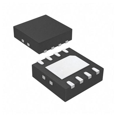
IC PWR SWITCH N-CHAN 1:1 8WSON


画像は参考用です.
製品の詳細については、「製品仕様」を参照してください。
IC PWR SWITCH N-CHAN 1:1 8WSON
200 ドル以上のご注文には、限定版の中華風のギフトがプレゼントされます.
1000 ドルを超える注文は、30 ドルの配送料免除の対象となります.
5000 ドルを超える注文では、配送料と取引手数料が免除されます.
これらのオファーは新規顧客と既存顧客の両方に適用され、2024 年 1 月 1 日から 2024 年 12 月 31 日まで有効です。.
TI
TPS22962DNYR datasheet
WSON-8
ICチップ
 Lead free/RoHS Compliant
今すぐ見積もりリクエストを送信してください。3 日以内に見積もりを提出する予定です。 5月 02, 2024。 今すぐご注文ください。以内に取引が完了する予定です。 5月 06, 2024。 追伸:時間はGMT+8:00に従います。


1 Features
• Integrated Single Channel Load Switch
• VBIAS Voltage Range: 2.5 V to 5.5 V
• VIN Voltage Range: 0.8 V to 5.5 V
• Ultra Low RON Resistance
– RON = 4.4 mΩ at VIN = 5 V (VBIAS = 5 V)
• 10 A Maximum Continuous Switch Current
• Low Quiescent Current
– (20 µA for VBIAS = 5 V)
• Low Shutdown Current
– (1 µA for VBIAS = 5 V)
• Low Control Input Threshold Enables Use of 1.2 V or Higher GPIO
• Controlled and Fixed Slew Rate Across VBIAS and VIN
– tR = 2663 µs at VIN = 5 V (VBIAS = 5 V)
• Quick Output Discharge (QOD)
• SON 8-Pin Package with Thermal Pad
• ESD Performance Tested per JESD 22
– 2-kV Human-Body Model (HBM)
– 1-kV Charged-Device Model (CDM)
2 Applications
• Servers
• Medical
• Telecom Systems
• Computing
• Industrial Systems
• High Current Voltage Rails
3 Description
The TPS22962 is a small, ultra-low RON, single channel load switch with controlled turn on. The device contains an N-channel MOSFET that can operate over an input voltage range of 0.8 V to 5.5 V and supports a maximum continuous current of 10 A.
The combination of ultra-low RON and high current capability of the device makes it ideal for driving processor rails with very tight voltage dropout tolerances. The controlled rise time of the device greatly reduces inrush current caused by large bulk load capacitances, thereby reducing or eliminating voltage droop on the power supply. The switch can be independently controlled via the ON pin, which is capable of interfacing directly with low-voltage control signals originating from microcontrollers or low voltage discrete logic. The device further reduces the total solution size by integrating a 224-Ω pull-down resistor for quick output discharge (QOD) when the switch is turned off.
The TPS22962 is available in a small 3.00 mm x 3.00 mm WSON-8 package (DNY). The DNY package integrates a thermal pad which allows for high power dissipation in high current and high temperature applications. The device is characterized for operation over the free-air temperature range of –40°C to 105°C.

Request a quote TPS22962DNYR at censtry.com. All items are new and original with 365 days warranty! The excellent quality
and guaranteed services of TPS22962DNYR in stock for sale, check stock quantity and pricing,
view product specifications, and order contact us:sales@censtry.com.
The price and lead time for TPS22962DNYR depending on the quantity required, please send your request to us,
our sales team will provide you price and delivery within 24 hours, we sincerely look forward to cooperating with you.
TI
115 PCS
AML3501 .PDF
TI
30 PCS
AMI808EZWT .PDF
TI
40 PCS
AMI808BZWT .PDF
TI
184 PCS
AM3352BZCZD30 .PDF
2024-05-01
worked fine thanks
2024-04-30
Fast delivery, good quality
2024-04-30
todo en perfectas condiciones gracias.
2024-04-29
Works perfect.Thanks
2024-04-27
Todo bien mas que contento. Gracias
2024-04-24
llego rápido y todo lo que pedí, de buena calidad.

皆様からのフィードバックを非常に重視しております。 最も誠実なレビューを共有してください。
*コメントを投稿する前にアカウントにログインしてください