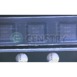
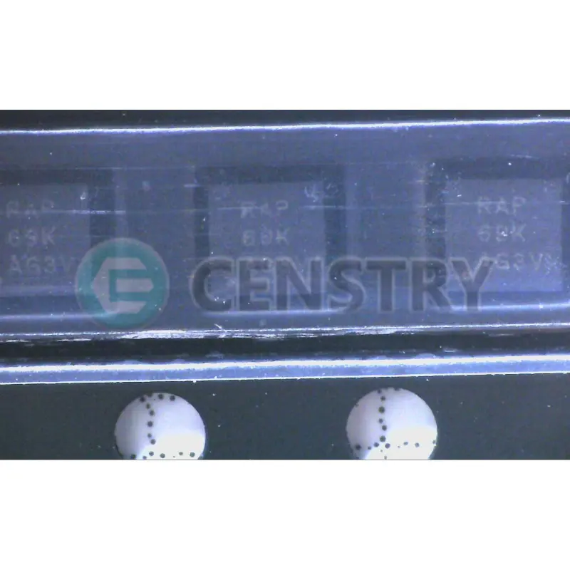
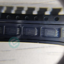
IC REG MULT CONFG ADJ 960MA 6SON


画像は参考用です.
製品の詳細については、「製品仕様」を参照してください。
IC REG MULT CONFG ADJ 960MA 6SON
200 ドル以上のご注文には、限定版の中華風のギフトがプレゼントされます.
1000 ドルを超える注文は、30 ドルの配送料免除の対象となります.
5000 ドルを超える注文では、配送料と取引手数料が免除されます.
これらのオファーは新規顧客と既存顧客の両方に適用され、2024 年 1 月 1 日から 2024 年 12 月 31 日まで有効です。.
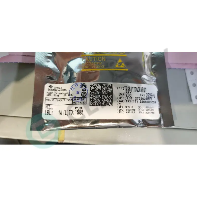
TI
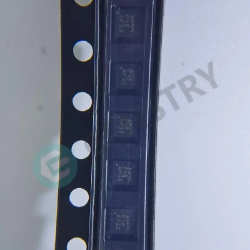
TPS61170QDRVRQ1 datasheet
WSON-6
ICチップ
 Lead free/RoHS Compliant
今すぐ見積もりリクエストを送信してください。3 日以内に見積もりを提出する予定です。 7月 28, 2024。 今すぐご注文ください。以内に取引が完了する予定です。 7月 31, 2024。 追伸:時間はGMT+8:00に従います。


FEATURES
• Qualified for Automotive Applications
• 3-V to 18-V Input Voltage Range
• High Output Voltage: Up to 38 V
• 1.2-A integrated Switch
• 1.2-MHz Fixed Switching Frequency
• 12 V at 300 mA and 24 V at 150 mA from 5-V Input (Typical)
• Up to 93% Efficiency
• On-The-Fly Output Voltage Reprogramming
• Skip-Switching Cycle for Output Regulation at Light Load
• Built-in Soft Start
• 6-Pin, 2 mm × 2 mm QFN Package
APPLICATIONS
• 5-V to 12-V and 24-V, 12-V to 24-V Boost Converter
• Buck Boost Regulation Using SEPIC Topology
DESCRIPTION
The TPS61170-Q1 is a monolithic, high-voltage switching regulator with integrated 1.2-A, 40-V power MOSFET. It can be configured in several standard switching-regulator topologies, including boost and SEPIC. The device has a wide input-voltage range to support applications with input voltage from multi-cell batteries or regulated 5-V, 12-V power rails.
The TPS61170-Q1 operates at a 1.2-MHz switching frequency, allowing the use of low-profile inductors and low-value ceramic input and output capacitors.
External loop compensation components give the user flexibility to optimize loop compensation and transient response. The device has built-in protection features, such as pulse-by-pulse overcurrent limit, soft start and thermal shutdown.
The reference voltage to which the FB pin regulates is 1.229V. The reference voltage can be lowered using a 1-wire digital interface (Easyscale™ protocol)
through the CTRL pin. Alternatively, a pulse width-modulation (PWM) signal can be applied to the CTRL pin. The duty cycle of the signal reduces the feedback reference voltage proportionally.
The TPS61170-Q1 is available in a 6-pin 2 mm × 2 mm QFN package, allowing a compact power-supply solution.

Request a quote TPS61170QDRVRQ1 at censtry.com. All items are new and original with 365 days warranty! The excellent quality
and guaranteed services of TPS61170QDRVRQ1 in stock for sale, check stock quantity and pricing,
view product specifications, and order contact us:sales@censtry.com.
The price and lead time for TPS61170QDRVRQ1 depending on the quantity required, please send your request to us,
our sales team will provide you price and delivery within 24 hours, we sincerely look forward to cooperating with you.
TI
8000 PCS
LMD18201T .PDF
TI
4470 PCS
INA240A3PWR .PDF
TI
62900 PCS
TPS7B8250QDRVRQ1 .PDF
TI
380948 PCS
TPS7B8150QDRVRQ1 .PDF
2024-07-27
Great ! Like always !
2024-07-26
We like, thank you
2024-07-26
Great value, as description, thanks :-)
2024-07-26
You should try him out if they show stk.
2024-07-25
We have been doing business with Censtry for several years now, both buying and selling. Every transaction has gone smooth. Todd is a true professional and knows how to do business right!
2024-07-23
Very professional, and timely, delivered exactly what they promised!!!
2024-07-19
Very good Seller
2024-07-11
Tina and her Sales Team are reliable, honest and professional.it is a pleasure to work with them.
2024-06-25
Thanks Mike
2024-05-24
Great company ,and the staff is friendly!

皆様からのフィードバックを非常に重視しております。 最も誠実なレビューを共有してください。
*コメントを投稿する前にアカウントにログインしてください