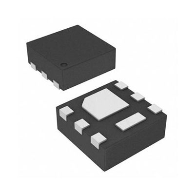
IC REG BOOST PROG 0.7A SYNC 6SON


画像は参考用です.
製品の詳細については、「製品仕様」を参照してください。
IC REG BOOST PROG 0.7A SYNC 6SON
200 ドル以上のご注文には、限定版の中華風のギフトがプレゼントされます.
1000 ドルを超える注文は、30 ドルの配送料免除の対象となります.
5000 ドルを超える注文では、配送料と取引手数料が免除されます.
これらのオファーは新規顧客と既存顧客の両方に適用され、2024 年 1 月 1 日から 2024 年 12 月 31 日まで有効です。.
TI
TPS61291DRVR datasheet
WSON-6
電源管理IC
 Lead free/RoHS Compliant
今すぐ見積もりリクエストを送信してください。3 日以内に見積もりを提出する予定です。 5月 02, 2024。 今すぐご注文ください。以内に取引が完了する予定です。 5月 07, 2024。 追伸:時間はGMT+8:00に従います。


1 Features
• Input Voltage Range 0.9V to 5V
• Startup Voltage 1.5V at 20mA Load
• Pin Selectable Output Voltages: 3.3V, 3V, 2.5V
• 15nA typical Quiescent Current in Bypass Mode
• 5.7μA typical Quiescent Current in Boost Mode
• Bypass Switch from VIN to VOUT
• IOUT > 200mA at 3.3V VOUT, VIN = 1.8V
• Internal Feedback Divider Disconnect (Bypass Mode)
• Controlled Bypass Transition Prevents Reverse Current into Battery
• Power-Save Mode at Light Loads
• Overtemperature Protection
• Redundant Overvoltage Protection
• Small 2mm x 2mm SON 6-pin package
2 Applications
• Metering (Gas, Water, Smart Meters)
• Remote Controls
• Home Security / Home Automation
• Single 3V Li-MnO2 or 2 x 1.5V Alkaline Cell Powered Applications
3 Description
The TPS61291 is a boost converter with pin selectable output voltages and an integrated bypass mode. In bypass operation, the device provides a direct path from the input to the system and allows a low power micro controller (MCU) such as the MSP430 to operate directly from a single 3V Li-MnO2 battery or dual alkaline battery cells.
In bypass mode the integrated feedback divider network for boost mode operation is disconnected from the output and the quiescent current consumption drops down to only 15nA (typical).
In boost mode the device provides a minimum output current of 200mA at 3.3V VOUT from 1.8V VIN. The boost mode is used for system components which require a regulated supply voltage and cannot directly operate from the input source. The boost converter is based on a current-mode controller using synchronous rectification to obtain maximum efficiency and consumes typically 5.7uA from the output. During startup of the boost converter, theVSEL pin is read out and the integrated feedback network sets the output voltage to 2.5V, 3V or 3.3V.
Bypass mode or boost mode operation is controlled by the system via the EN/BYP pin. The device integrates an enhanced bypass mode
control to prevent charge, stored in the output capacitor during boost mode operation, from flowing back to the input and charging the battery.
The device is packaged in a small 6-pin SON package (DRV) measuring 2.0mm × 2.0mm x 0.75mm.


Request a quote TPS61291DRVR at censtry.com. All items are new and original with 365 days warranty! The excellent quality
and guaranteed services of TPS61291DRVR in stock for sale, check stock quantity and pricing,
view product specifications, and order contact us:sales@censtry.com.
The price and lead time for TPS61291DRVR depending on the quantity required, please send your request to us,
our sales team will provide you price and delivery within 24 hours, we sincerely look forward to cooperating with you.
TI
115 PCS
AML3501 .PDF
TI
30 PCS
AMI808EZWT .PDF
TI
40 PCS
AMI808BZWT .PDF
TI
184 PCS
AM3352BZCZD30 .PDF
2024-05-02
Excellent fast postage
2024-05-01
Ware dankend erhalten!
2024-05-01
Tested ALL OK!!!
2024-05-01
Excellent ***** Highly recommended - Thank you.
2024-04-30
Worked like a charm... thanks
2024-04-29
Llegó bien
2024-04-26
Would use Iceberg again. Good response to enquiry and requests.
2024-04-21
Great! recommended !
2024-04-10
We are very pleased with our business with her, and look to give her every PO we can. Thanks Dusty.
2024-03-20
Very reliable and delivered as promised. Mark and Wendy, great job! Thanks again.

皆様からのフィードバックを非常に重視しております。 最も誠実なレビューを共有してください。
*コメントを投稿する前にアカウントにログインしてください