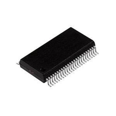
IC GATE DRVR HALF-BRIDGE 10VSON


画像は参考用です.
製品の詳細については、「製品仕様」を参照してください。
IC GATE DRVR HALF-BRIDGE 10VSON
200 ドル以上のご注文には、限定版の中華風のギフトがプレゼントされます.
1000 ドルを超える注文は、30 ドルの配送料免除の対象となります.
5000 ドルを超える注文では、配送料と取引手数料が免除されます.
これらのオファーは新規顧客と既存顧客の両方に適用され、2024 年 1 月 1 日から 2024 年 12 月 31 日まで有効です。.
TI
UCC27282DRCR datasheet
UCC27282DRCR
RF集積回路
 Lead free/RoHS Compliant
今すぐ見積もりリクエストを送信してください。3 日以内に見積もりを提出する予定です。 5月 06, 2024。 今すぐご注文ください。以内に取引が完了する予定です。 5月 09, 2024。 追伸:時間はGMT+8:00に従います。


1 Features
• Drives Two N-Channel MOSFETs in High-Side Low-Side Configuration
• 5-V Typical Under Voltage Lockout
• Input Interlock
• Enable/Disable Functionality
• 16-ns Typical Propagation Delay
• 12-ns Rise, 10-ns Typical Fall Time With 1800-pF Load
• 1-ns Typical Delay Matching
• Absolute Maximum Negative Voltage Handling on Inputs (–5 V)
• Absolute Maximum Negative Voltage Handling on HS (–14 V)
• 3.5-A Sink, 2.5-A Source Output Currents
• Absolute Maximum Boot Voltage 120 V
• Low Current (7-µA) Consumption when Disabled
• Integrated Bootstrap Diode
• Specified from –40°C to 140°C Junction Temperature
2 Applications
• Telecom and Merchant Power Supplies
• Motor Drives and Power Tools
• Auxiliary Inverters
• Half-Bridge and Full-Bridge Converters
• Active-Clamp Forward Converters
• High Voltage Synchronous-Buck Converters
• Class-D Audio Amplifiers
3 Description
The UCC27282 is a robust N-channel MOSFET driver with a maximum switch node (HS) voltage rating of 100 V. It allows for two N-channel MOSFETs to be controlled in half-bridge or synchronous buck configuration based topologies. Its 3.5-A peak sink current and 2.5-A peak source current along with low pull-up and pull-down resistance allows the UCC27282 to drive large power MOSFETs with minimum switching losses during the transition of the MOSFET Miller plateau. Since the inputs are independent of the supply voltage, UCC27282 can be used in conjunction with both analog and digital controllers.
The input pins as well as the HS pin are able to tolerate significant negative voltage, which improves system robustness. Input interlock further improves robustness and system reliability in high noise applications. The esnable and disable functionality provides additional system flexibility by reducing power consumption by the driver and responds to fault events within the system. 5-V UVLO allows systems to operate at lower bias voltages, which is necessary in many high frequency applications and
improves system efficiency in certain operating modes. Small propagation delay and delay matching specifications minimize the dead-time requirement which further improves efficiency. Under voltage lockout (UVLO) is provided for both the high-side and low-side driver stages forcing the outputs low if the VDD voltage is below the specified threshold. An integrated bootstrap diode eliminates the need for an external discrete diode in many applications, which saves board space and reduces system cost. UCC27282 is offered in a small package enabling high density designs.

Request a quote UCC27282DRCR at censtry.com. All items are new and original with 365 days warranty! The excellent quality
and guaranteed services of UCC27282DRCR in stock for sale, check stock quantity and pricing,
view product specifications, and order contact us:sales@censtry.com.
The price and lead time for UCC27282DRCR depending on the quantity required, please send your request to us,
our sales team will provide you price and delivery within 24 hours, we sincerely look forward to cooperating with you.
TI
115 PCS
AML3501 .PDF
TI
30 PCS
AMI808EZWT .PDF
TI
40 PCS
AMI808BZWT .PDF
TI
184 PCS
AM3352BZCZD30 .PDF
2024-05-05
Joe is very professional and helpful. We recommend CENSTRY as a business partner.
2024-05-05
It is a gerat pleasure to work with Joanne
2024-05-05
JEFF IS THE HOOK-UP, GOOD SERVICE, LOW PRICES
2024-05-04
Keith and the staff at Censtry are a plessure to deal with, thank you for all your business. Chris
2024-05-03
Linda is the best and rocks. Thank you for your support. Hardy
2024-04-30
Mati and group are great to work with!
2024-04-25
Mr. Jordan, Quick, efficient, reliable seller !
2024-04-14
Nice smooth transaction
2024-03-24
One of the good companies in China to provide good quality, original parts. always pleasure dealing with
2024-02-10
as promised! Derek is professional!

皆様からのフィードバックを非常に重視しております。 最も誠実なレビューを共有してください。
*コメントを投稿する前にアカウントにログインしてください